 MENU
MENU 

Egg-carton-style patterning keeps charged nanoparticles in place and suitable for a wide range of applications
Researchers at the University of Michigan and Seoul National University of Science and Technology have devised a new method for manufacturing devices that require precisely sized and positioned micro- and nanoscale particles. The technique is suitable for a wide array of assembly of micro- and nanoscale objects, and useful for electronic devices, and biological applications.
“It’s very hard to regulate things in the microscopic and nano-scale. You want the particles to sit there, and they won’t,” said Jay Guo, project leader and professor of electrical engineering and computer science. “We found a way to sort and localize large quantities of particles, and we can do it in a very scalable fashion.”
With this ability, engineers would be able to more efficiently manufacture and assemble photonic crystals, filtration devices and biological assays, create more sensitive sensing devices, and much more.
Guo has been working in the area of nanomanufacturing for decades, beginning with his work on roll-to-roll nanoimprint lithography. He switched to the current methodology of nanopatterning relying only on a sliced silicon wafer because of its relative simplicity and speed.
The new method adds an electric charge, which seems to make all the difference.
Creating the microfluidic device
The goal of this research was to end up with a layer of orderly and like-sized micro- or nanoparticles that could be integrated into a device with high-density arrays. Current methods for doing this tend to be tedious while requiring complicated structures. Or, they are best suited for particles that are 10s to 100s of micrometers, leaving the separation and sorting of sub-micrometer particles a persistent challenge.
Guo and his international team of researchers, including former student Prof. Jong G. Ok, put together a microfluidic device that achieved their desired goals using a method that is also scalable, and relatively low cost. Ok’s team has been continuing to push the inscribing technology at his institute in Korea
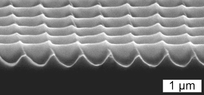
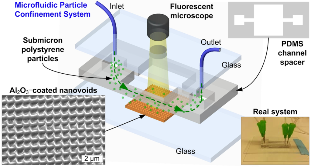
The heart of the device is a specially designed substrate that captures the particles of a specific size in an orderly arrangement. To do this, the researchers first created indentations, in the shape of nanovoids, into a polycarbonate substrate through a patterning technique known as dynamic nanoinscribing (DNI). The resulting nanovoids were all the same size.
The substrate is then coated with Al2O3 and given a positive charge after being immersed in a salt solution.
Figure 1 shows the test setup, which allows for submicron-sized fluidic particles to enter the system and flow over the substrate before exiting. These particles are negatively charged in order to increase their attraction to the positively-charged nanovoids in the substrate. They were also given fluorescent labels for easy detection.
It might be expected that most of the particles would simply fall to the bottom of the fluid and rest on the substrate, but that’s not what happened.
Instead, only those of a specific size rested in the nanovoids. Three distinct sizes of particles were injected into the system: 200nm, 500nm, and 1,000nm (or 1𝜇m). As shown in Figure 2, the 200nm particles were least successful in finding a home in the nanovoid indentations, and the 1𝜇m particles were only slightly more successful, but both cases are not stable.
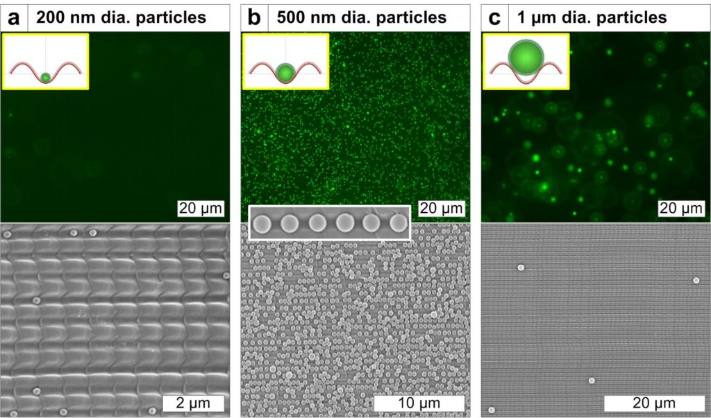
500nm was the sweet spot. As more and more particles of this size were attracted to their final resting places in the nanovoid wells, the overall energy in the system decreased (in technical terms, this was due to the electrostatic attraction and increased entropy from the freed ions), which helped keep the particles strongly nested in their wells.
Guo described his delight in discovering that the nested particles could not be easily dislodged, even after rinsing the channel with water. It took sonication, or strong sound energy, being applied to the particles to dislodge them.
The researchers also tested what would happen when: 1) the substrate was completely flat, with no nanovoids, and no charge; 2) the substrate was flat but given a charge; 3) the substrate was imprinted with the nanovoids, but not charged. None of these situations provided the desired result.
Future possibilities
A key aspect of the technique for creating these nanovoids is its scalability. The 2D-DNI process creates specifically-sized nanovoids at high speed (~1 m/min or faster), which easily beats the competition by an order of magnitude. It is also a relatively low-cost technique.
While Guo’s primary focus was the application of this technique to building ever-shrinking and high-density electronic systems, he believes it could also have an impact on the future of biomedical devices, as well as the ability of medical researchers to investigate proteins, cancer cells, and bacteria interacting with charged surfaces.
Additional Information
The research was detailed in “Size-Selective Sub-micrometer-Particle Confinement Utilizing Ionic Entropy-Directed Trapping in Inscribed Nanovoid Patterns,” by Long Chen, Ashwin Panday, Jonggab Park, Mingyu Kim, Dong Kyo Oh, Jong G. Ok, and L. Jay Guo, ACS Nano 2021 15(9).
Device fabrication was accomplished in the Lurie Nanofabrication Facility.
Guo has several U.S. patents related to development of the manufacturing process, and declares competing financial interest specifically in US Patent, No. 10,661,273, by Jong G. Ok, Lingjie J. Guo, Long Chen, and Ashwin Panday.
Guo is also affiliated with mechanical engineering, macromolecular science & engineering, and applied physics. Ok is a professor of mechanical and automotive engineering at Seoul National University of Science and Technology.