 MENU
MENU 

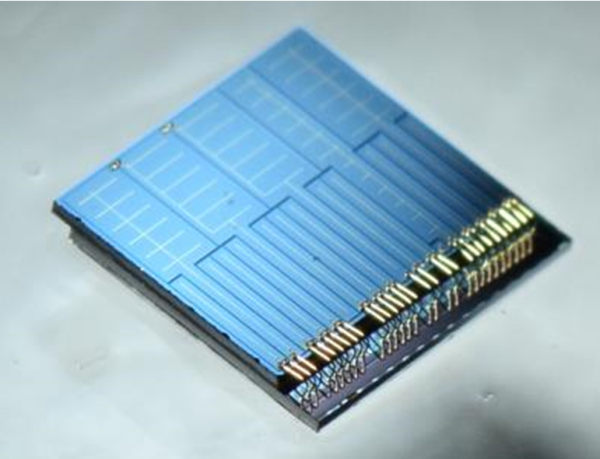
The Lurie Nanofabrication Facility
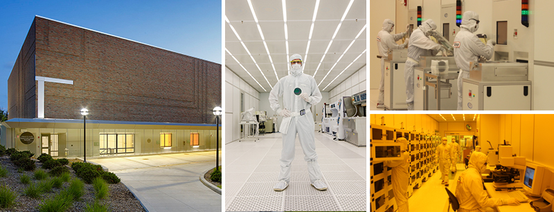
 Enlarge
Introduction
The Lurie Nanofabrication Facility is a world-class facility that serves the entire University of Michigan as well as researchers around the world. Each year, approximately $55M in technology-advancing research happens in an environment that is so clean, in some parts there are no particles larger than 0.3 microns – which is about the size of the smallest bacterial cell.
It was built to facilitate next-generation research in semiconductor device and circuit fabrication, integrated microsystems and MEMS technologies, and broad areas of nanotechnology including nanoelectronics, nanophotonics, and nanobiotechnology. The LNF also allows researchers to explore new materials for applications ranging from healthcare to national security.
Research conducted in the LNF has led to:
- improved neural probes for treatment of Parkinson’s and other diseases;
- novel methods to uncover the mysteries of the brain;
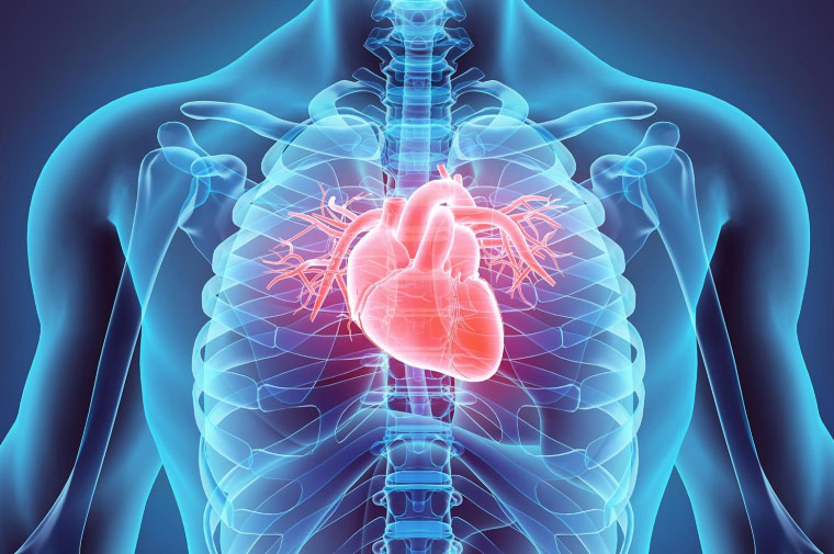
- implantable medical devices, such as arterial stents with integrated sensors;
- nanoscale lasers;
- improved cochlear implants for the treatment of hearing loss;
- transparent and flexible electronics;
- high-efficiency lighting;
- integrated microsystems for the Internet of Things;
- next generation solar cells;
- next generation memory devices;
- neuromorphic computing circuits;
- devices for weapons detection and medical imaging;
- new materials such as carbon nanotube coating for cloaking
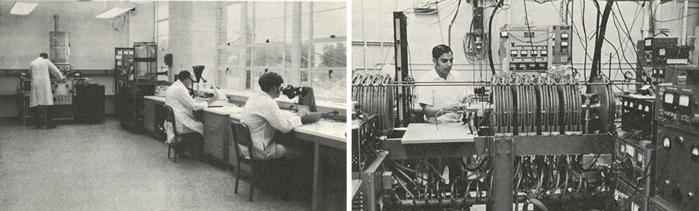
The LNF is the culmination of 70 years of steady advancements in device fabrication techniques at Michigan, beginning with the Electron Tube Laboratory (ETL). Back then, cutting-edge device fabrication could be accomplished in very “dirty” environments.
1946-59: Electron Tube Laboratory: Humble Beginnings
Michigan icon William Gould Dow organized the Electron Tube Laboratory (ETL) in 1946 with funding from the U.S. Army Signal Corps. Dow had been working at Harvard for the war effort, developing magnetrons and traveling wave fields for radar systems.
The Corps sponsored research into the behavior of microwave magnetron oscillators, which resulted in well-equipped microwave measurement and electron tube laboratories in the new East Engineering addition. By today’s standards, it was humble at best.
As alumnus and former lab director Nino Masnari (BSE MSE PhD EE ’58 ’59 ’64) recalled: “It was a classroom converted to a lab, which would not have been approved today in terms of safety. But we made devices that actually worked, and we were able to teach students how to fabricate devices. I told them even if it didn’t work, they could see what they were learning in classes. So even the failed experiments were valuable for learning. Not as good for research though.”
In the early 1950’s, former department chair and eventual NAE member Joseph E. Rowe(BSE MSE PhD EE ’51 ’52 ’55; and BSE Math ’51) developed an important new theory regarding traveling-wave amplifiers, and developed the Crestatron, a new type of high-efficiency, high-power microwave amplifier.
Rowe and others later developed a Poisson cell and analog computer system for the design of electron injection systems. That system was installed at the U.S. Army Electronics Command Laboratories.
 Enlarge
1958-1984: Electron Physics Laboratory
When Rowe became lab director in 1958, the lab was renamed Electron Physics Laboratory (EPL) to reflect a growing emphasis on solid-state devices and plasmas. Research at this time focused on microwave electron tube devices, gaseous plasmas, and semiconductors. Under his leadership, the Electron Physics Laboratory became one of the premier laboratories on campus.
Rowe was one of the major pioneers in the area of microwave devices, especially vacuum tube devices such as traveling wave tubes and magnetrons. These devices are still in wide use today in many applications, including high-power communication and radar systems as well as microwave ovens. His 1965 book, Nonlinear Electron Wave Interaction Phenomena, became a standard in the field.
George I. Haddad (BSE MSE PhD EE ’56 ’58 ’63), Robert J. Hiller Professor and former student of William Gould Dow, was named lab director when Rowe became the department chair in 1968. Haddad developed the first X-band traveling-wave ladder line ruby MASER (Microwave Amplification by Stimulated Emission of Radiation), which was a forerunner of the modern laser.
The MASER was one of the most significant solid-state devices of the time, and remains an important element in the amplification of microwave signals. Haddad also developed a cavity MASER that was placed on Peach Mountain to receive signals from outer space.
He also advanced the state of the art of Impact Avalanche Transit Time (IMPATT), BARITT, and Gunn self-oscillating mixers for Doppler radar applications, microwave sensors, automotive radars, intrusion alarms, and door openers.
These achievements were accomplished through some very difficult circumstances.
In the mid 1960’s, deciding that tubes were passe and solid state devices were the future, the Department of Defense abruptly stopped all funding of microwave research. Haddad’s first responsibility as lab director was the unhappy task of laying off several individuals who could no longer be supported, and also to reduce the level of graduate student support.
Betty Cummings, former lab and department administrator, recalled the many hours Haddad spent on the phone with colleagues and granting agencies to ensure the future of the lab. His efforts paid off.
We rebuilt the whole place, and it’s been growing ever since. We never had to lay off another person.
George Haddad
Prof. Haddad transformed the lab from one based on microwave tubes to one that supported solid-state electronics, and Michigan has remained a leader in solid-state devices and integrated circuits ever since. He was named a member of the National Academy of Engineering, “For contributions to microwave electronics and for leadership in electrical engineering research and education.”
By the 1970’s, according to Haddad, “There was not a single microwave company at the time that didn’t have a Michigan graduate.”
Nino Masnari, who led the lab from 1975-1979, presented the features of the lab at a special conference in the 1970’s for schools that had similar facilities. He said, “People were actually impressed with what we had at Michigan and what we were able to do. And at Michigan, students gained valuable experience doing the fabrication themselves, unlike some other schools who had technicians doing the work.”
Masnari left Michigan in 1979 to become department chair at NC State University, and later Dean of Engineering (1996-2006). His successor as lab director, Kensall D. Wise, became the next pivotal leader in the history of the LNF.
Wise arrived at Michigan in 1974. He recalled, “The Lab was new but primitive, and the furnaces were table-top units. But it was good enough for early sensor work and was a place to start. In those days, the principal function of lab coats was to keep your clothes clean.”
 Enlarge
Wise brought an entirely new area of research to Michigan, one focused on integrated circuits and sensors. He developed the course Integrated Circuits Laboratory, which allowed undergraduate students into the lab for their class projects. One of the 1976 class projects was to design and build a 64-bit SRAM chip.
“Sensors were a good match for our early lab in East Engineering,” said Wise. “They were in their formative stage, so the research didn’t require a lot of high tech equipment. Also, Michigan was a great place to do the interdisciplinary work required of sensor research.”
 Enlarge
Thirty years later, the technology was more complex and the facilities were much better but the goal was still to give students a look at the development of a complete chip.
Wise was one of the early leaders in establishing a new field known as microelectromechanical systems, or MEMS.
In 1976, Wise created what was perhaps the first silicon pressure sensor with on-chip readout circuitry. It was also the first micromachined sensor developed at Michigan.
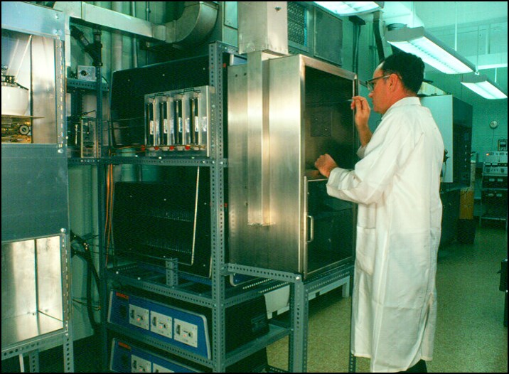
1978-1986: Transformation into a Modern Cleanroom
By the late 1970s, Wise was reaching a wall in what could be accomplished with the current facilities. With funding from the University and major gifts of equipment from industry, the lab began a process of expansion and renovation.
Wise was able to acquire additional new and used equipment for the lab in the early 1980’s, including used furnaces, hoods, a new mask aligner, and a Nitrox APCVD reactor.
“Things were a lot better, but we still occasionally found pigeon feathers in the furnace loading zones!” said Wise.
 Enlarge
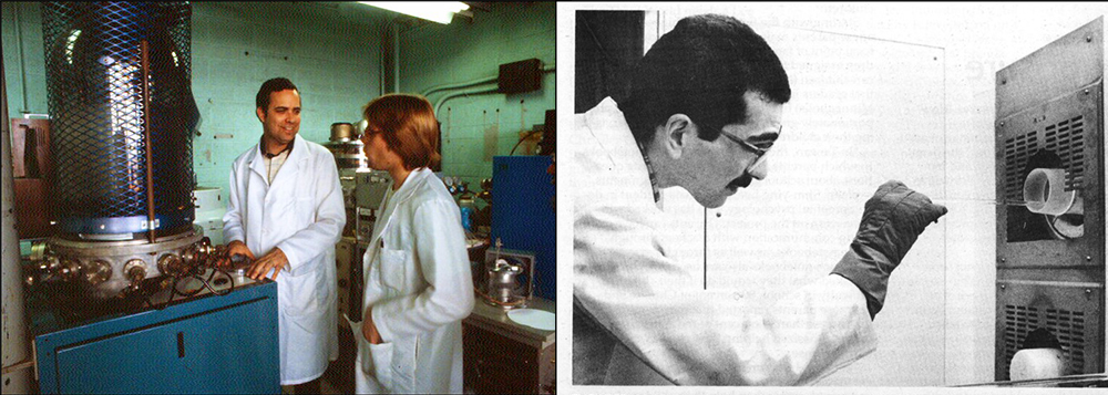 Enlarge
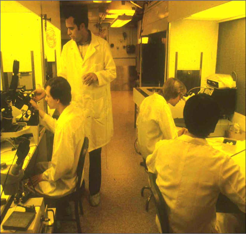
A clear picture of the type of research that was happening in the lab could be found in a 1980-81 publication: Solid-State Electronics at the University of Michigan.
Wise wrote in the introduction, “By the end of the 1970s, integrated electronics was having profound impacts on areas such as health care, telecommunications, transportation, consumer products, defense, and industrial process control. … Universities have a key role to play in this continuing revolution, both in terms of training the individuals who will carry it forward and in terms of performing basic research on which future progress depends.”
Students who used the Electron Physics Lab were specializing in solid-state electronics and learning to design, build, and test computers. Courses were being planned in VLSI computer design. Research focused on solid-state materials; microwave and millimeter-wave devices and circuits; and solid-state circuits and sensors.
As Director, it was Wise’s job to make sure the lab was sufficient not only for current, but future research. By the early 1980’s, this was not the case.
“Even with some newer equipment,” said Wise, “we were barely holding our own with respect to other university fabrication facilities. To remain competitive, we needed a lot more. But to get a real processing facility a number of things had to fall into place.”
What Wise meant by a “real processing facility” was a cleanroom.
Cleanroom facilities were relatively new to academia in the 1980’s. The first was built by Cornell in 1981 with NSF funding. This set the bar, and cleanrooms quickly became essential to academic research in solid state devices, integrated circuits, and all areas of micro and nanotechnology.
But they were extremely expensive, and it was tough times in the State of Michigan.
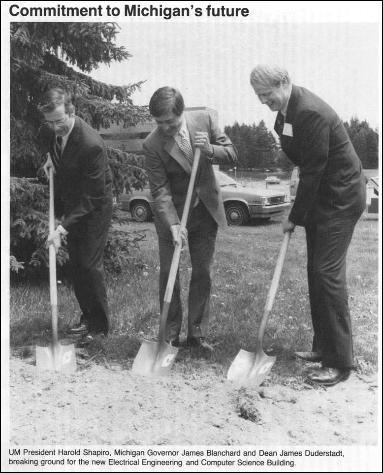
Fortunately, the University appointed the visionary James J. Duderstadt as Dean of Engineering in 1981. Duderstadt worked with the State of Michigan to fund the Electrical Engineering and Computer Science Building on North Campus, which included a true cleanroom facility.
The new lab was absolutely pivotal to our future work in Solid State and MEMS. Without it, none of our later successes would have been possible.
Ken Wise
And the opportunities for significant research breakthroughs were huge.
In 1981, Wise became director of a new program that would run for 25 years, funded by the National Institute of Neurological Disorders and Stroke (NINDS). This program enabled groundbreaking research in neural probes. David Anderson and Spencer BeMent were key researchers in this program.
 Enlarge
In 1984, the same year as the groundbreaking for the new building and lab, Michigan was selected by the Semiconductor Research Corporation (SRC) to lead a program in automated semiconductor manufacturing.
This program ran until 1998, and was named a Center of Excellence for Advanced Manufacturing Sciences by the late 1980’s. Directed by Wise, the overarching goal of the Center was to advance the manufacture of microcircuitry.
Wise was quoted as saying the following in a 1984 press release, “We’re talking about packing perhaps 100 chips, or circuits, on a single five-inch diameter wafer. To reach these nearly invisible dimensions, we’ve reached a point where some of the older technology is beginning to give. We have to shift to basically new process techniques.”
What does a cleanroom do?
1. Controls temperature (68 degrees +- 1 degree) and humidity (42.5% +- 2.5% relative humidity) to ensure that the chemicals, devices, and tools are not disturbed.
2. Controls ambient lighting. White light exposes the photosensitive films used to define the layers of monolithic solid-state devices and circuits, so cleanrooms are illuminated by yellow light.
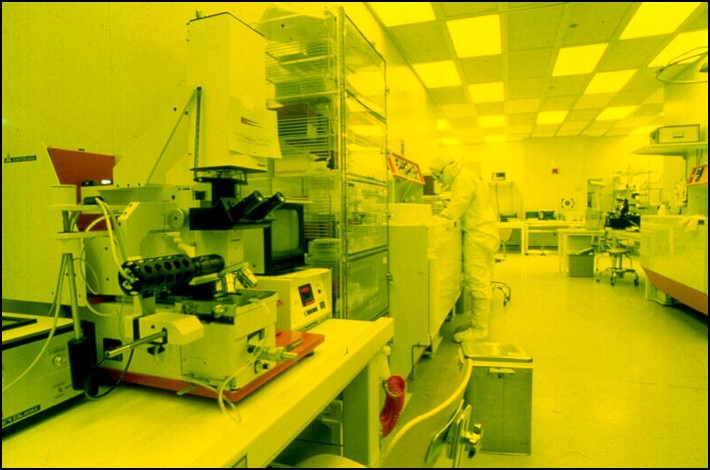
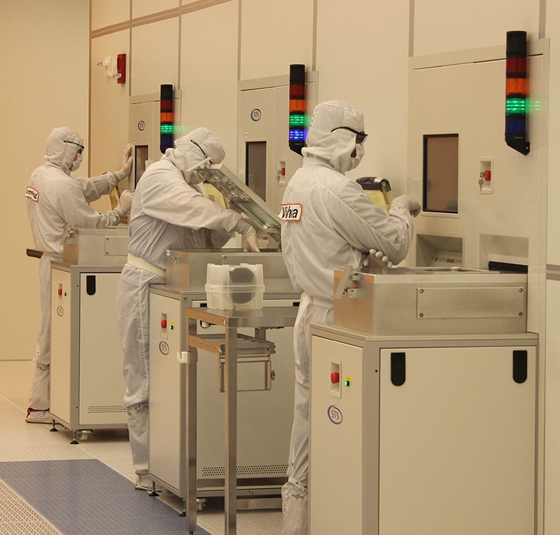
3. Cleans the air. The air is constantly recycled so that in a Class 10 room there are no more than 10 particles larger than .3µ in a cubic foot. The SSEL also includes rooms of Class 100, 1,000 and 10,000, that latter being used for student courses. A Class 10,000 room is sufficient for an operating room. A typical day outside is more like Class 10,000,000.
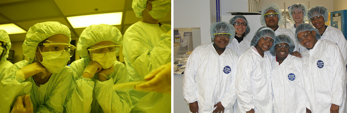
Lab users wear special “bunny suits” over their clothing and cover their head, hands, and feet to protect the devices from particles naturally emitted from their body and clothing. The smallest devices require the cleanest (Class 10) environment.
The lab is capable of features down to 10 nm (nanometers), which is thousands of times smaller than a human hair.
1986-2008: Solid-State Electronics Laboratory
The new 6,000 sq. ft. Laboratory, and U-M’s first cleanroom facility, was opened in the Fall of 1986. To reflect its new emphasis on solid state devices, the Electron Physics Laboratory had been renamed the Solid State Electronics Laboratory (SSEL) in 1984, at the time the Department of Electrical and Computer Engineering became the Department of Electrical Engineering and Computer Science.
 Enlarge
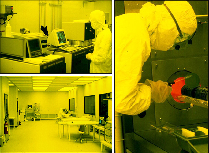 Enlarge
Haddad recalled that when the lab was built, it was essentially empty, and the equipment needed to move it to the next level was extraordinarily expensive. Fortunately, Haddad, Wise, and Associate Dean Chuck Vest (who later became Dean and Provost, and President of MIT) wrote a successful proposal to the State of Michigan to establish a Research Excellence Fund. This fund outfitted the SSEL with the equipment needed to fulfill its promise.
Additional support came from a $20M research center called the Center for High Frequency Microelectronics (CHFM), established in 1986 and directed by Haddad. The CHFM lasted 15 years, and opened new research avenues including state-of-the-art millimeter wave integrated circuits, sub-0.1-micron field-effect transistor technology, advanced epitaxial growth technologies, optoelectronic devices and integrated circuits, and quantum-based electronic devices and circuits.
The ability Michigan now had, thanks to the SSEL, to produce microwave integrated circuits led to the first university courses on the subject. In addition, the Center’s pioneering efforts in quantum-based optoelectronic devices and systems put Michigan at the leading edge of technology that even now, nearly three decades later, remains at the forefront of engineering research.
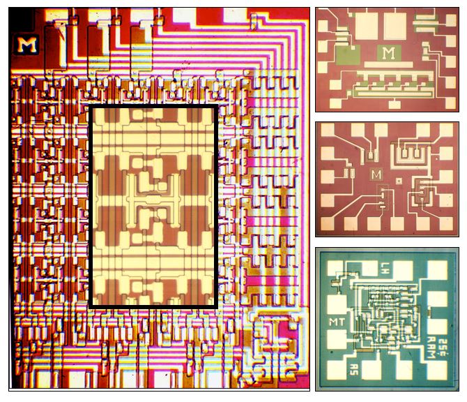
Impact of Quantum Dot Technology
 Enlarge
Leading the effort in quantum-based optoelectronic devices was Pallab Bhattacharya, Charles M. Vest Distinguished University Professor and James R. Mellor Professor of Engineering. Bhattacharya, who served as Lab Director from 1991-1998, was named a member of the National Academy of Engineering for his contributions to quantum-dot optoelectronic devices and integrated optoelectronics.
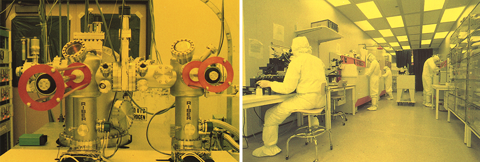
When he came to Michigan in 1984, Bhattacharya brought the first molecular beam epitaxy (MBE) machine used for academic research in the State. The only other MBE system was in the Ford Scientific Research Lab, and it was used solely to make lasers for automobile sensors. An MBE is used to grow materials atom by atom.
Much of Bhattacharya’s groundbreaking research is founded on his discovery in 1988, with colleague Jasprit Singh, of a new technique for growing unique semiconductor structures, which came to be known as self-assembled quantum dots.
 Enlarge
Following the discovery of self-organized quantum dots, Bhattacharya and colleagues at Michigan, namely Rachel Goldman (Materials Science and Engineering), Ted Norris, Brad Orr (Physics), and Jasprit Singh, illuminated the phenomenon through rigorous testing and further experimentation. Michigan was 7-10 years ahead of the research community in this area, and in the coming decades Bhattacharya established Michigan as a premier institution in optoelectronics research.
Prof. Bhattacharya and others, including Jasprit Singh, Jamie Phillips (a graduate student at the time), and Ted Norris were among the first to report room temperature operation of a quantum dot laser in 1996. Subsequent research established the quantum dot laser as the best semiconductor laser available in terms of performance characteristics.
In the mid 1990’s, Bhattacharya led the development of a unique approach to photoreceivers, which is now used in virtually all contemporary high-performance photoreceivers. These photoreceivers are used in industry today as optical fiber communication links.
MEMS, Microsystems, and the Michigan Probe
Alongside the efforts of Haddad, Bhattacharya, and others in semiconductors, microwaves, optoelectronics, and related research, Wise was expanding his influence in MEMS and Microsystems. He was later elected a member of the National Academy of Engineering for his contributions to sensors and microelectromechanical systems.
MEMS was coalescing as a distinct discipline in the early 80’s, marked by newly-formed conferences in the field. Wise and his colleagues were heavy players early on in the MEMS-focused Transducers conference, which was initiated in 1981, and he was instrumental in establishing the Solid-State Sensors, Actuators and Microsystems Workshop, first held in 1984.
Those were years in which the field was taking shape. We were doing pioneering work with the goal of being the world’s center for MEMS.
Ken Wise
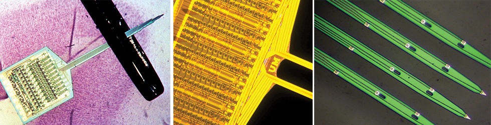
This work included groundbreaking research in neural probes, flowmeters, gas sensors, pressure sensors, infrared detectors, and other MEMS devices – all developed in the SSEL.
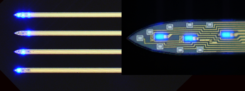
The neural probe research was so wide-ranging, the devices came to be known simply as the “Michigan Probes.” These are probes that go into tissue and can be used to measure the actual electrical signals in the brain itself. [Read more about the Michigan Probes]
 Enlarge
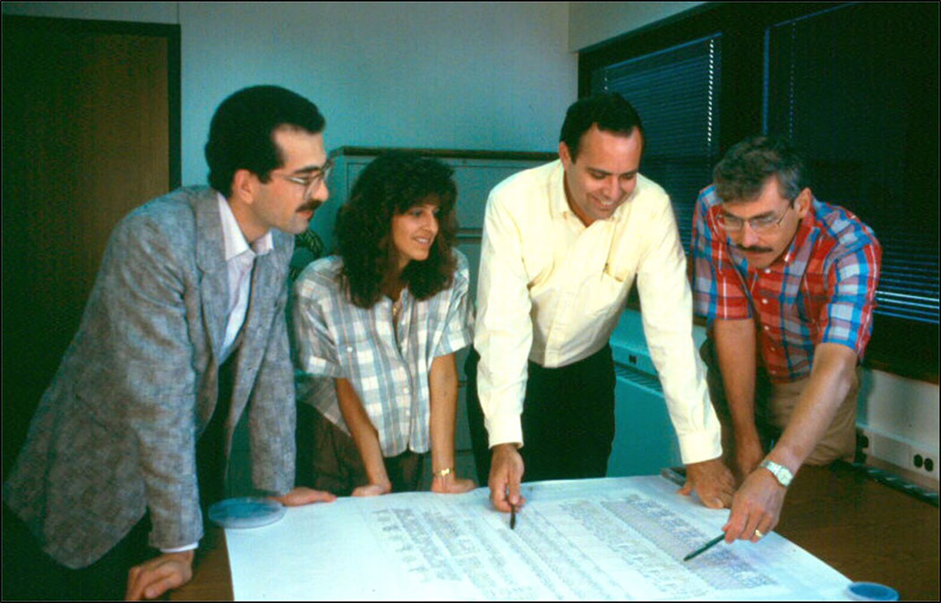 Enlarge
Between 1992 and 2006, Michigan provided over 7500 probes in more than a hundred different designs to researchers worldwide. Journals and conferences dedicated to neural interfaces sprang from this and related work.
Michigan researchers developed a wide array of probes for such purposes as: researching neurological diseases, learning how biological systems work, stimulating muscles, or stopping tremors due to Parkinson’s Disease. They also developed probes that could reside inside the human body for long periods of time.
When DARPA formed its MEMS activities in the early 1990’s, one of the first programs funded was a project proposed by Prof. Wise and his former student-turned-colleague Khalil Najafi (Peter and Evelyn Fuss Chair of Electrical and Computer Engineering and Schlumberger Professor of Engineering). Their plan was to develop a wristwatch-sized device that combined sensors and a microprocessor, and importantly, that was also wireless.
This research provided the foundation for the NSF Engineering Research Center, called the Center for Wireless Integrated Microsystems (WIMS), established in 2000 and led by Wise, with Najafi serving as Deputy Director.
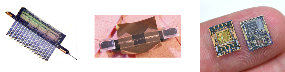
Between 2000-2010, faculty in the WIMS Center developed neural interfaces, smart stents for improved cardiovascular care, biopsy needles capable of measuring local tissue density as an aid in diagnosing cancer, intraocular pressure sensors for treating glaucoma, thin-film-based cochlear electrode arrays for restoring hearing to the deaf, hand-held breath analyzers for detecting the biomarkers of tuberculosis and lung cancer, wristwatch-size radiation detectors for ensuring the safety of containerized shipping, air-quality monitors for protecting the global environment, and a record low-power microcontroller. It also authored 59 patents, and was the foundation for 12 startup companies. [Read more about WIMS]
 Enlarge
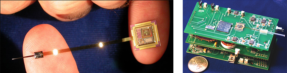 Enlarge
1998 – 2008: Planning the Lurie Nanofabrication Facility: What it Takes to Be the Best
In 1998, Dean Stephen Director initiated a strategic planning process for the next major fundraising campaign. Khalil Najafi, who had just been named Director of the SSEL, was asked to prepare a presentation about the significance of nanotechnology and microsystems for a college-wide retreat.
Every department presented a few ideas, and faculty voted on which areas for the future they deemed extremely important for the future.
Nanotechnology and microsystems was considered one of the most important by all of the faculty, along with biomedical engineering and computing. This was the start.
Khalil Najafi
And then there was the WIMS ERC.
In 1999 we put in the Letter of Intent. And we said if we get funded, we’ll expand the lab.
Khalil Najafi
They were funded in 2000, and shortly thereafter the first feasibility plans for the new lab began. By this time, the equipment in the Lab was over 15 years old, and replacement parts were not even available for many tools.
Three key lab staff – Dennis Grimard, Dennis Schweiger, and Timothy Brock – took an active role in designing the lab. This trio came to be known as DDT. Their input was absolutely critical to the final design and ultimate success of the lab, which was referred to as the most complex undertaking ever attempted at the University of Michigan by the head of U-M’s Plant Department. Grimard was later recruited to help design MIT’s new cleanroom facility.
 Enlarge
Groundbreaking occurred in 2005, but the plans were far from finalized. Najafi was planning a long-awaited sabbatical, and Prof. Fred Terry was appointed Director of the SSEL. Terry was also Chair of the SSEL Expansion Committee, a committee established in 2004 to ensure the proper planning of the new Lab.
Having arrived at Michigan in 1985 as an assistant professor, Terry saw firsthand the gap between promise and reality in the brand new lab. As good as the SSEL was when it was built in 1986, there were problems that regularly interrupted the research in the lab.
It seemed that the SSEL did great about 10 months out of the year, but the heating and cooling equipment couldn’t handle the extremes in Michigan’s weather.
There were days when processes just didn’t work, either because the temperature was off by a degree, or the humidity was too high in the summer, or too low in the winter.
Fred Terry
Terry was determined to fix existing problems and make sure nothing similar happened in the new lab. To complicate matters further, the University was recruiting Prof. Stephen Forrest to Michigan.
Forrest was already a world leader in optoelectronics, and a member of the National Academy of Engineering for advances in optoelectronic devices, detectors for fiber optics, and efficient organic LEDs for displays.
Bringing his lab [which took 9 semi trucks to transport from Princeton] to Michigan meant the current lab space would need to be renovated alongside the expansion.
One of the many items to be negotiated with the College and University was the cost of connecting the air flow process in the new Lab with the existing Lab. At a price tag of half a million dollars, it seemed like an easy line item to cut. But it was one of many line items that Terry, DDT, and even the Deans fought to keep in the budget, which was already seriously in the red.
Thanks to their success over that one item, Michigan now has 13,500 sq. ft. of absolutely reliable cleanroom space instead of half that much.
It doesn’t sound very dramatic. But one of the things that makes Michigan’s Lab one of the best in the country is – IT WORKS.
Fred Terry
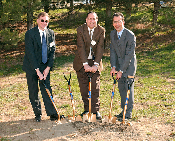
Progress in the world of micro and nano does not come cheap. A key supporter of the lab was Ann Lurie, long-time supporter of Prof. Wise’s research with its direct application to healthcare. She launched the fundraising effort with a $15M gift, and many others stepped up to ensure completion of the $40M expansion and renovation. Another $20M in equipment from the University completed the facility.
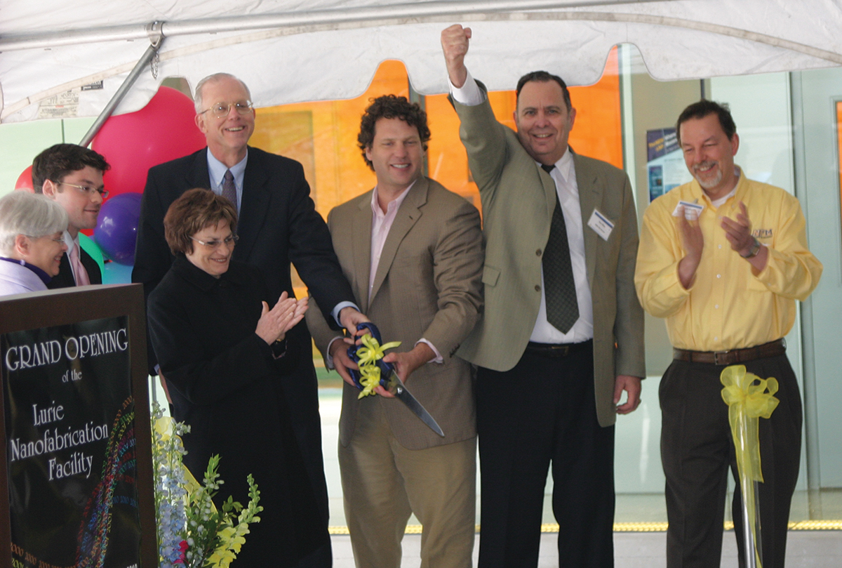 Enlarge
At the dedication of the newly-named Robert H. Lurie Nanofabrication Facility (LNF) in 2008, Wise told the crowd that he was as excited as anyone to see what future breakthroughs would be accomplished at Michigan thanks to the facility and the synergy of the faculty and students.
“The microsystems now being developed are creating new electronics that will become truly pervasive in solving many of the critical problems of this new century.” said Wise. “It will help us preserve the environment, improve health care, protect our national and global infrastructure, provide homeland security, and improve the discovery, generation, distribution, and use of energy.”
With the renaming and dedication of the facility, oversight of the LNF was transferred from Electrical and Computer Engineering to the College of Engineering. This was a financial necessity.
According to managing director Dr. Sandrine Martin, “As feature sizes go from microns to submicrons to nanometers, the scale of the investment that’s needed to allow research to happen at that level becomes large and generally too much for a single group, or even a department to support. These types of facilities generally have to move out to larger groups, like a College of Engineering, which happened in our case, or a university-wide office of Research.”
2004-2015: National Nanotechnology Infrastructure Network (NNIN): The Transition to a User-Friendly Facility
In 2004, right in the middle of planning for the expansion, the Lab became a member of the National Nanotechnology Infrastructure Network (NNIN). The NNIN was an NSF-funded partnership of 14 user facilities across the country that provided training, education, and outreach activities, as well as programs on societal and ethical issues involving nanotechnology.
 Enlarge
Najafi served as Director of NNIN until the program ended in 2015.
According to Martin, participation in the NNIN marked a dramatic shift in the lab. “We went from primarily a research lab with a smaller community in which everyone participates, to one that is more of a service organization,” she said.
This shift was one envisioned by Najafi as early as 1996, when he began talking about changing the way fees were collected in the Lab to be more equitable to all users, especially those who didn’t use the lab very much.
When he became Director of the SSEL in 1998, Najafi continued the transition.
“The main thing we had to do was change this lab from a super specialized lab to a lab that was flexible and could respond to changing demands very quickly,” said Najafi.
He started to hire more highly-skilled technical lab staff who understood the processes and could specialize in certain areas. His first key hire was former SSEL/LNF Managing Director and U-M alumnus Dr. Dennis Grimard.
Najafi and Grimard started the process of automating the lab, and put an even greater emphasis on safety as they envisioned more outside users in the lab.
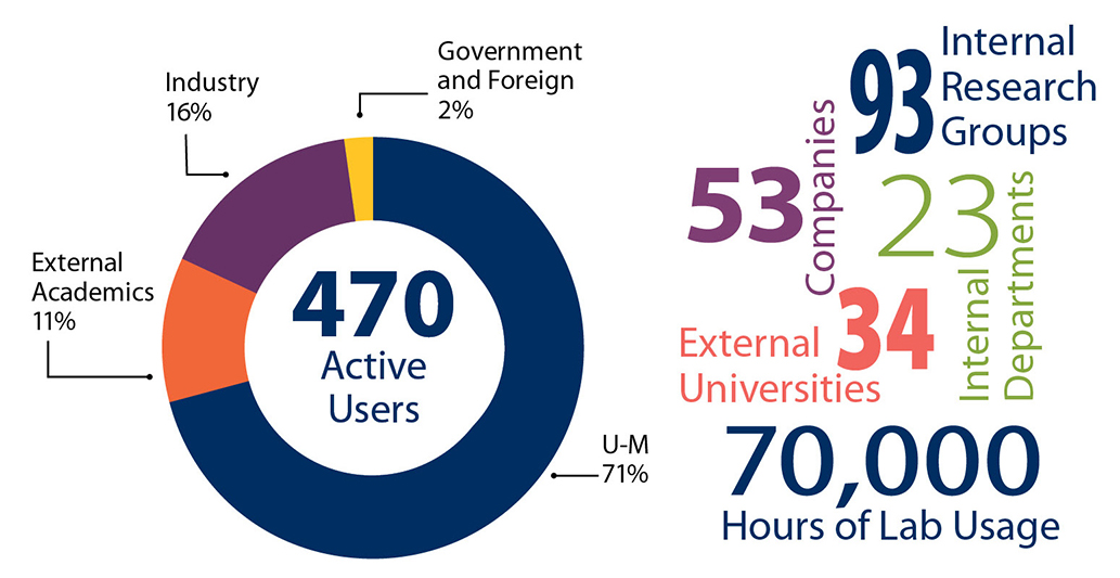
The number of users in the facility grew from more than 100 in the mid 1990s to more than 500 at its peak, with 35% of the users coming from outside the University.
 Enlarge
According to Najafi, there is a healthy tension between the Lab as a research facility and a user facility, but it is the research that drives the future.
“On one of my first DARPA projects,” said Najafi, “we bought the first DRIE tool, and possibly the first bonder. At that time only a few people needed them. Now over time many more people have adopted that technology and are using this tool – not just for building sensors but for a whole range of things. The only way to be ahead of the game is to make sure the lab is equipped for the future. Research tells you the way of the future.”
 Enlarge
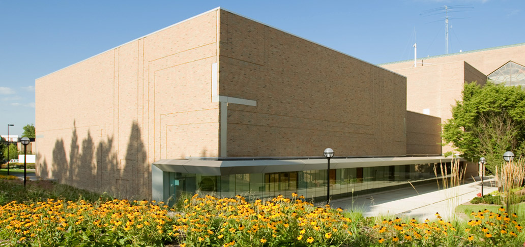 Enlarge
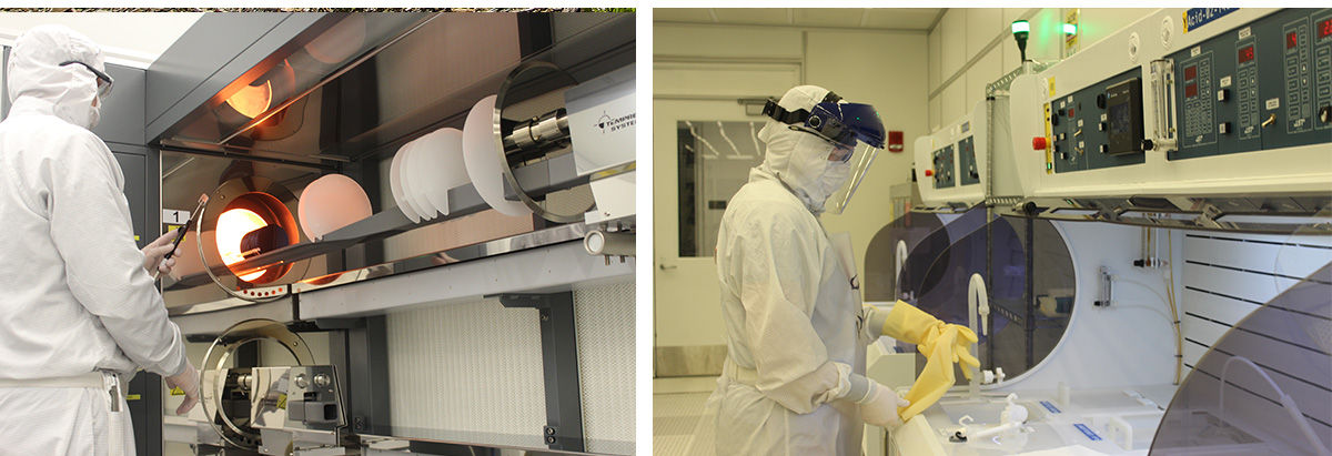 Enlarge
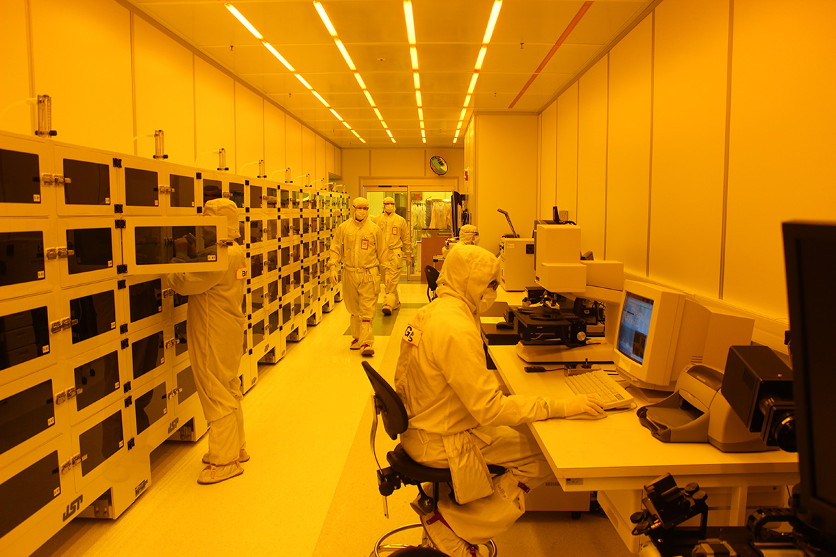 Enlarge
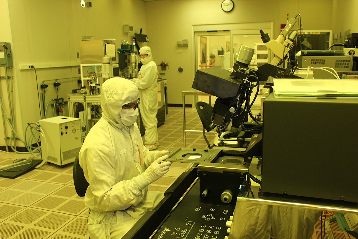 Enlarge
In recent years, close to 500 individuals make use of the LNF annually. Most are U-M researchers from within the College of Engineering, as well as the Cancer Center, Pediatrics, Psychology, Computation, Medicine & Bioinformatics, and more. The remaining users came from local startup companies, larger corporations, government agencies, and other universities.
The core users of the lab continue to be researchers in solid state devices & nanotechnology, and MEMS & Microsystems – areas that have their roots in the former ETL, EPL, and SSEL.
The current Director, Wei Lu, says the scale of the LNF combined with its variety of tools make it unique among academic nanofabrication facilities.
“Most any major capability one can think of, we have it here,” said Lu. “The LNF offers extensive expertise and equipment that cover most every aspect of semiconductor research, from materials growth and individual process developments to systems level integration. We often heterogeneously integrate different components to form a functional system that is more powerful than any single device in the system.”
The LNF has established technologies for bulk and surface micromachining, MEMS fabrication, electrical, optical, biomedical and energy device fabrication, and MEMS-CMOS integration. Equipment is available for thin film deposition and growth, optical and e-beam lithography, nanoimprinting, wet and dry etching, electrochemical deposition, chemical mechanical planarization, wafer bonding, wafer dicing, wire bonding, metrology, and more.
In addition to pure research, the LNF offers a broad range of expertise and equipment to support high impact education, research and business development activities.
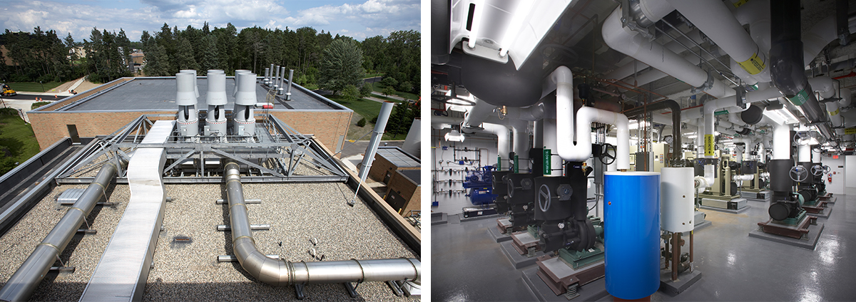
Behind the Scenes
To be a true production-type cleanroom you need lots of air, lots of ultra-pure water, and lots of exhaust, said Dennis Schweiger, who is currently responsible for the smooth functioning of the LNF. “We have all that,” said Schweiger. “So no matter what the research is going to be over the next 20-25 years, we should have enough capacity to handle it.”
Maintaining exact particle, humidity, and temperature settings for each area of the 13,500 sq. ft. of cleanroom requires an astonishing 65,000 sq. ft. of infrastructure support.
About 110,000 cubic feet per minute of air is pushed into the cleanroom. It’s pressurized to keep the dirt from coming in, and the air is circulated. As air is lost, fresh air from the outside is brought it – which needs to be brought to the correct temperature and humidity, and then filtered. Huge fans on the roof help with this process.
 Enlarge
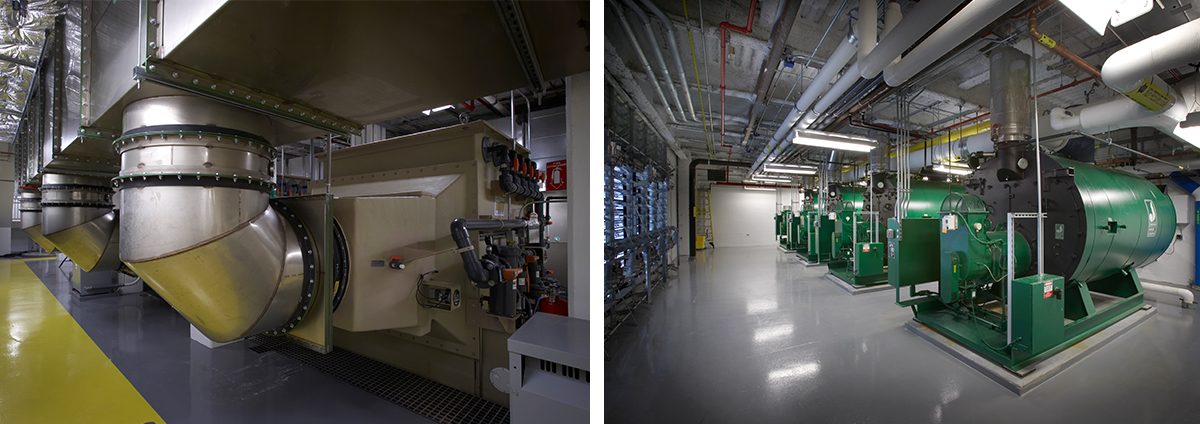 Enlarge
For those who run the lab, this area is almost as exciting as the more public face of the lab; it is certainly as important.
The DDT team took great care in how this area was laid out, and is a source of great pride for past and current lab staff. Even a former U-M Provost was given a tour of the gigantic fans on the roof.
Safety in the Lab
Times have changed since the early 80’s, when an APCVD tool that ran on 100% silane had a pipe that ran to the roof where the exhaust burned off with a yellow flame.
Today there’s a safety system that monitors hundreds of details to make sure the lab is operating safely at all times, and there is a 24-hr on call system.
Schweiger said, “We have a million and a half dollars invested in a gas detection system. It’s brand new as of June 2017 and protects everyone in the building.”
This new system is not there to correct existing problems. There have been no leaks in the lab. It’s there because lab safety is paramount at Michigan’s LNF. Staff work tirelessly to ensure everyone’s safety not only in the lab, but those who work in the building, and those who simply visit from time to time.
 Enlarge
Current Research
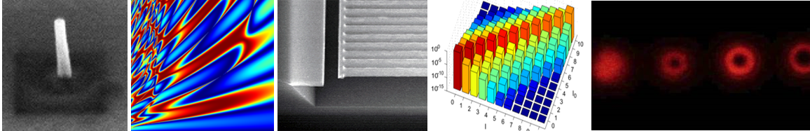
Following is a description of just a few of the projects going on in the LNF as of 2017.
 Enlarge
Wei Lu conducts research in emerging electrical devices such as resistive random-access memory (RRAM), neuromorphic circuits, and nanowire transistors. His research has resulted in the successful startup company, Crossbar, Inc., which is now delivering commercial memory products to customers. His group has developed computer chips that have the potential to process complex data, such as images and video orders of magnitude faster and with much less power than today’s most advanced systems. In related research, he has created a computing system made with memristors that can dramatically adapt to the environment and the task on hand to achieve maximal efficiency with minimal power.
I couldn’t do much without the LNF, except for simulations. All of my research projects depend critically on this facility.
Wei Lu
 Enlarge
Stephen Forrest conducts research on organic LEDs, as well as photovoltaic cells, and lasers & optics. His technology is found in devices that are pervasive in the marketplace, including Samsung smart phone displays. More recently, Prof. Forrest and his team achieved an efficient, deep, display quality blue using PHOLEDs that comes close to meeting the stringent brightness requirements of the National Television Systems Committee. His team also discovered a way to increase PHOLED efficiency by 50% for use in general lighting. He was a member of a team that devised a way for solar cells to capture more sunlight while being placed on rooftops and other pitched surfaces, and is currently involved in research that may lead to the ability to grow new heart tissue for cardiac patients.
 Enlarge
Euisik Yoon is leading an NSF Technology Hub to better understand how the brain works. His own group is building light-emitting diodes as small as neurons to measure how changes in the activity of a single neuron can affect its neighbors. The advances in knowledge and neural implant technology could lead to better prosthetics and treatments for conditions like Parkinson’s disease, deafness, blindness, paralysis and depression. In other research, he has developed a new kind of microfluidic chip that can capture rare, aggressive cancer cells for improved understanding of how cancer spreads in a collaboration with researchers from eight different departments and four different institutions around the world. He is also building microfluidic systems for the detection of prostate cancer.
 Enlarge
Khalil Najafi conducts research in micromachined sensors, microelectromechanical systems (MEMS) and integrated microsystems. He has made lasting contributions in several different areas of microsensors, including fabrication and packaging technologies, inertial sensors, energy harvesters, implantable biomedical sensors, and integrated electronics for implantable neural prostheses. He has also accomplished seminal work in MEMS-based power sources. In recent research, he and his group are building a navigation device that doesn’t need any external frame of reference, so that the gyroscope is meant to guide navigation devices without using GPS. The devices are slated for use in the guidance systems of missiles, satellites and unmanned aerial vehicles.
 Enlarge
Pallab Bhattacharya conducts research in compound semiconductor heterostructures as well as quantum dot lasers and detectors, optoelectronic integrated circuits, nanophotonic and spintronic devices, visible LEDs and lasers. He has made dramatic advancements in quantum dot lasers that are expected to find applications in solid-state lighting, full color mobile projectors, optical data storage, and even medical and military applications. More recently, he created a near-equilibrium room temperature Bose-Einstein condensate, a scientific milestone that opens up entirely new avenues of research and is expected to lead to increasingly sensitive instrumentation and measurements; and he demonstrated an electrically injected polariton laser, which scientists have been trying to accomplish since the device was first proposed in 1996.
 Enlarge
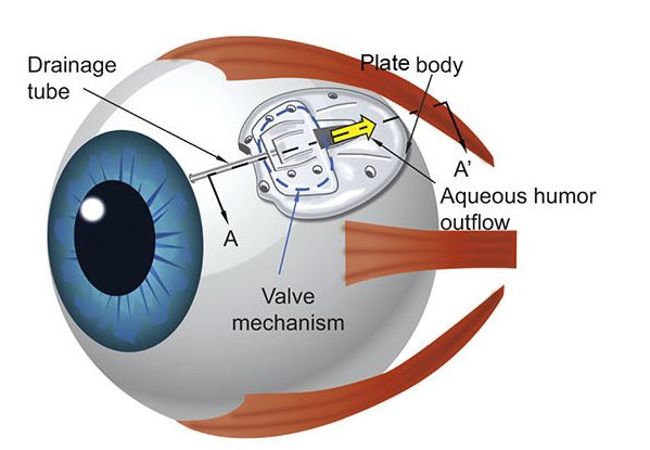
Yogesh Gianchandani focuses his research in MEMS. His research interests include all aspects of design, fabrication, and packaging of micromachined sensors and actuators and their interface circuits. He has blended work in materials, processes, and device structures, to form a wide variety of new devices, including biomedical devices (active cardiovascular stents, wireless MEMS actuators for the treatment of glaucoma, biliary stents, biopsy needles), microGeiger counters, very high-temperature pressure sensors, Knudsen pumps, microfluidic devices, new microfabrication processes that can be used for wireless sensing systems, and a microfabricated gas chromatograph for detection of a wide variety of chemicals and indoor pollutants.
 Enlarge
Jay Guo uses the lab to create structural colors that can provide unusual visual effects without using colored pigments, with a wide range of applications such as colored coatings, displays, and imagers. He researches flexible transparent conductor technologies that will benefit flexible displays, improved solar cell and LED efficiencies; related to this he achieved the thinnest, smoothest layer of silver that can survive air. He researches optoacoustic transducers that provide non-invasive and high-precision therapeutics while minimizing damage to healthy tissues. And he has developed nanolithography technologies that use UV light rather than very expensive excimer lasers or EUV light sources.
 Enlarge
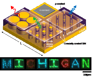
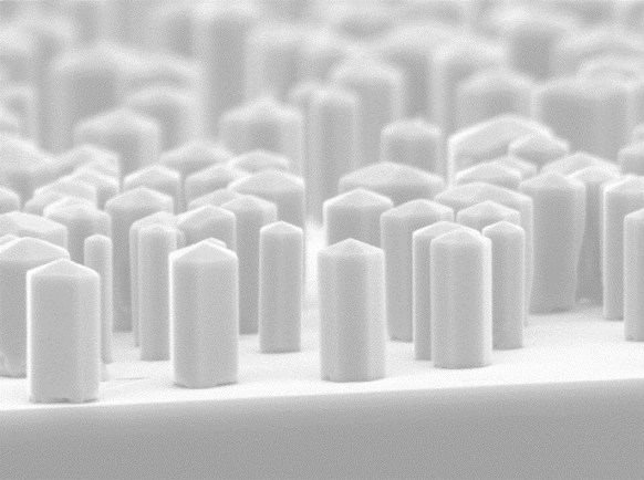
P.C. Ku investigates nanophotonic devices and related nanofabrication techniques with the goal of improving the efficiency of optoelectronic devices and systems. Applications include energy efficient lighting and renewable energy, data communication and signal processing, data storage, display, biomedical diagnosis, and quantum information science. He and his group recently created an LED-based microdisplay built on gallium nitride nanostructures. This microdisplay offers high brightness for outdoor use without sacrificing long-term stability and power efficiency. Microdisplays are critical components in augmented reality applications.
 Enlarge
Zetian Mi uses the LNF to develop new photocatalysts and photoelectrodes to convert sunlight, water, and carbon dioxide to hydrogen and hydrocarbon fuels. He is also developing UV light emitters which can be used for water purification and disinfection, and can potentially replace mercury lamps to enable a solid-state UV revolution.
 Enlarge
Jamie Phillips is investigating optoelectronic materials for the next generation of infrared detectors, photovoltaics for solar energy generation and energy harvesting, and thin film electronics. Infrared detectors are of high importance for a variety of defense, scientific, and commercial applications. His group has built energy harvesting devices for extremely low-power computing systems used for Internet of Things applications.
 Enlarge
Hui Deng, a faculty member in the Physics Department, works on controlling light-matter interactions in semiconductors to create novel many-body quantum systems with applications to future quantum photonic technologies.
The resources at the LNF, both hardware and the technical expertise in the LNF community, is indispensable.
Hui Deng
Companies in the LNF
Following is a list of some of the companies that have used the LNF recently and in the past to help develop their products. Several companies are Michigan startups.
Accuri Instruments
Adobe
Dexter Research Center, Inc.
Discera
ePack
Evigia Systems
First Solar
HandyLab
Integrated Sensing Systems
MEMStim
Midwest MicroDevices
Mobius Microsystems
Nanoselect
NeuMoDx Molecular, Inc.
NeuroNexus Technologies
PicoCal, Inc.
Picometrix, Inc.
Promerus
Quantum Opus
Sonetics Ultrasound, Inc.
Structured Microsystems
Stryker
Toyota Technical Center
Translume
The Future
The LNF is a tool to tackle the global challenges of the 21st century, including:
- Sustainability through efficient lighting and solar cells
- Health: Glaucoma, Epilepsy, Deafness, Blindness, Paralysis, Cardiovascular Disease, Parkinson’s Disease, Diabetes, Brain research, Cancer detection and treatment
- Intelligent Electronic Systems
- Ubiquitous Sensing for Internet of Things
- Environmental Monitoring Systems
- Infrastructure Monitoring for Buildings, Bridges, and Other Structures
- Monitors for Food and Resource Production
Thanks to visionary leaders, generous donors, expert staff, and a University committed to its mission, the LNF stands ready to serve society and enhance technological breakthroughs for the next generation.